Bruce Pocket Lab: A Custom ESP32-S3 Handheld
- ESP32-S3 (N8R8)
- ST7735 1.8" TFT
- PlatformIO
- C/C++
- NRF24L01+ 2.4GHz
- PN532 NFC/RFID
- NEO-6M GPS
- 2N2222 IR Driver
- TP4056 + MT3608 (J5019)
- 18650 Li-ion
- SPI & I²C
Bruce Pocket Lab: A Custom ESP32-S3 Handheld
Adapting open-source Bruce firmware for a custom ESP32-S3 N8R8 hardware platform: integrating a 1.8-inch ST7735 SPI display, designing a five-button tactile navigation system with long-press escape logic, routing modular RF, NFC, IR, and GPS peripherals, and building a self-contained rechargeable power system.
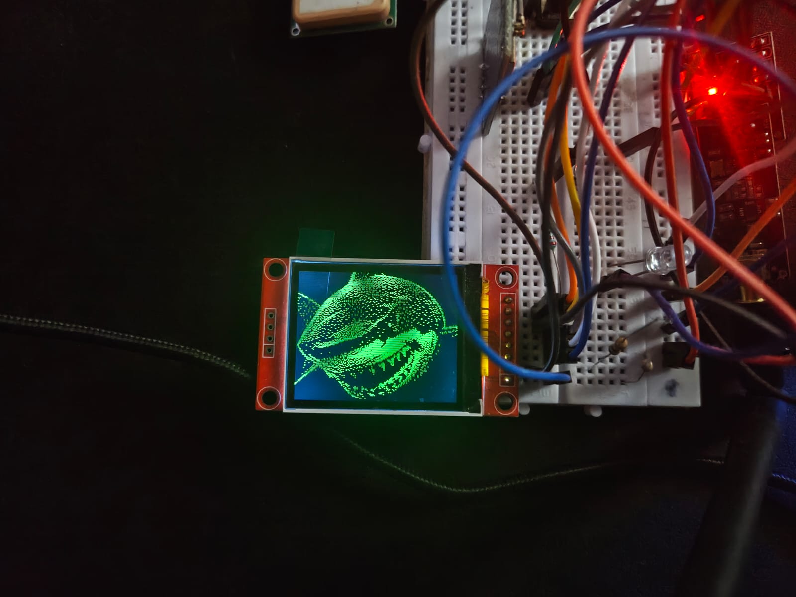
⚡ Project Overview & Engineering Objectives
The Bruce Pocket Lab is an ongoing hardware and firmware engineering project to create a portable, standalone embedded multi-tool. While commercial security and diagnostic handhelds exist, they are either closed proprietary devices or built around rigid hardware configurations. The goal of this project is to take the versatile open-source Bruce firmware ecosystem and adapt it to an accessible, high-performance physical build constructed from discrete breakout modules and custom firmware definitions.
The foundation of the device is the ESP32-S3 N8R8 microcontroller, which delivers dual-core 32-bit Xtensa processing at 240 MHz alongside 8 MB of on-chip Flash and 8 MB of Octal PSRAM. Around this core, the project interfaces a 1.8-inch ST7735 color TFT display, a 5-button tactile navigation pad, an NRF24L01+ 2.4 GHz radio, a PN532 NFC/RFID transceiver, a NEO-6M GPS receiver, a high-current infrared transmitter/receiver circuit, and an 18650 Li-ion power subsystem with active voltage sensing.
What I Am Building and Why
- Hardware-Specific Adaptation: Rather than relying on generic pre-compiled binaries, this project maintains a dedicated board definition (
boards/esp32-s3-st7735/) and PlatformIO build pipeline tailored to the exact pinout and timing characteristics of my hardware. - Ergonomic 5-Button Navigation: Embedded devices without full QWERTY keyboards or touchscreens often struggle with navigation. I designed and tested a 5-button physical input scheme (UP, DOWN, LEFT, RIGHT, SELECT) where a time-delayed hold on the SELECT button triggers Back/Escape (
BTN_ESC), avoiding the need for a bulky sixth button. - Coexistence of Multiple High-Speed Buses: Connecting SPI, I²C, UART, analog sensing, and GPIO interrupts on a single microcontroller requires strict bus isolation, shared SPI chip-select coordination, and clean power distribution.
- Open Engineering Documentation: Every step—from initial breadboard bring-up through debugging power drops and verifying GPS NMEA sentence parsing—is captured in the repository with Fritzing diagrams, pinout configurations, and build logs.
Current Status: IN PROGRESS. The breadboard prototype stage was completed on 27 September 2026 with the successful generation and hardware flashing of the merged 4.29 MB firmware binary. The next phase focuses on transitioning from solderless breadboard to a permanent perfboard assembly and custom 3D-printed enclosure.
🔌 System Architecture & Master Wiring
The overall hardware topology interconnects seven subsystems to the ESP32-S3. All connections have been validated on breadboard against the pinout configuration files in the repository (brucePins.conf and pinout.txt).
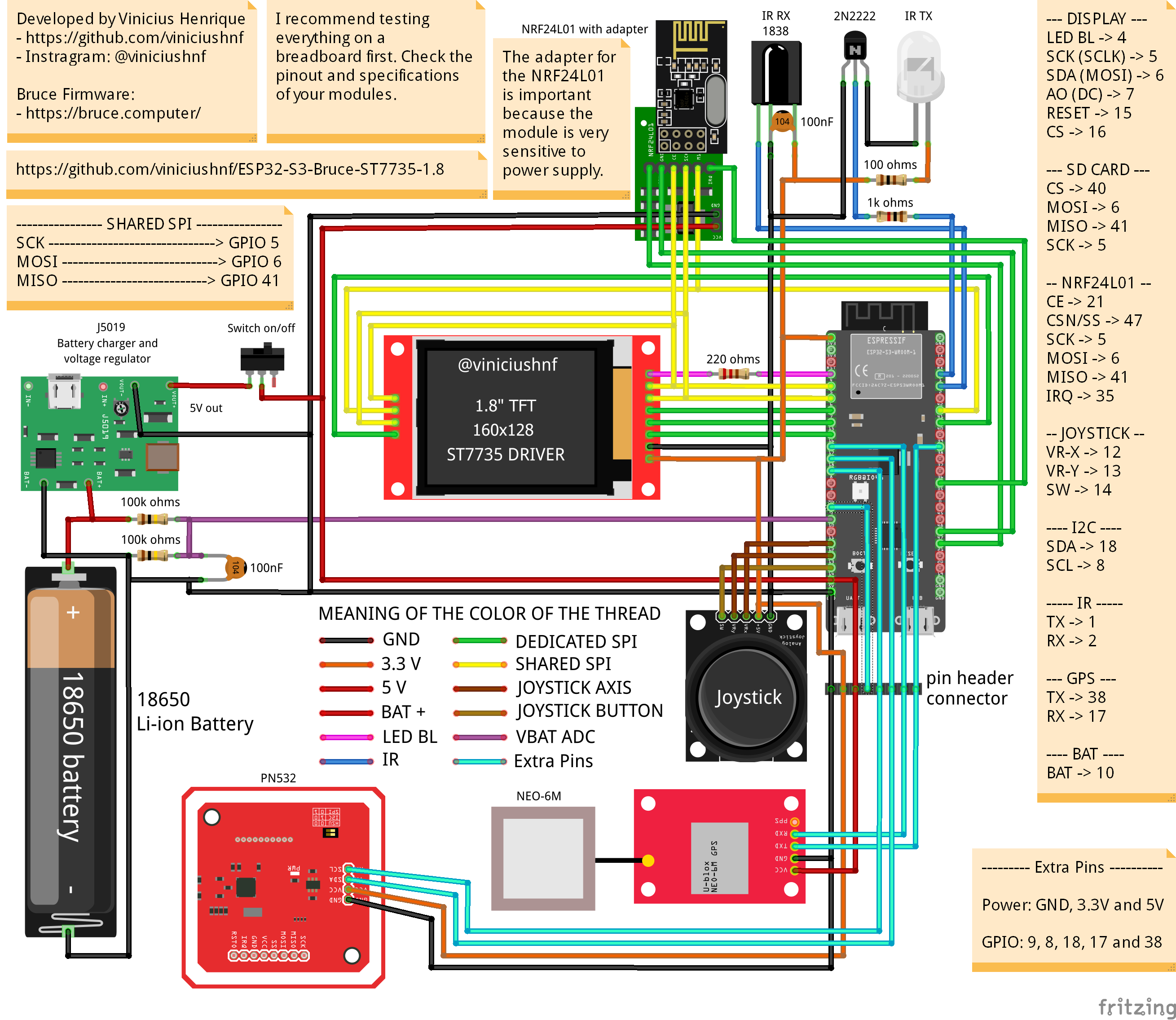
Master Pinout Configuration
| Module | Module Pin | ESP32-S3 GPIO | Bus / Signal Type | Electrical Notes |
|---|---|---|---|---|
| ST7735 Display | LED BL | GPIO 4 | GPIO Output | Backlight enable (active high) |
| ST7735 Display | SCK (SCLK) | GPIO 5 | Shared SPI Clock | Clock line shared with SD card & NRF24 |
| ST7735 Display | SDA (MOSI) | GPIO 6 | Shared SPI MOSI | Master Out Slave In |
| ST7735 Display | A0 (DC) | GPIO 7 | Control Output | Data / Command register select |
| ST7735 Display | RESET | GPIO 15 | Control Output | Hardware display reset line |
| ST7735 Display | CS | GPIO 16 | SPI Chip Select | Dedicated display chip select (active low) |
| MicroSD Card | CS | GPIO 40 | SPI Chip Select | Dedicated SD card select |
| MicroSD Card | MISO | GPIO 41 | Shared SPI MISO | Master In Slave Out (shared with NRF24) |
| NRF24L01 Radio | CE | GPIO 21 | Control Output | Chip Enable (activates RX/TX modes) |
| NRF24L01 Radio | CSN / SS | GPIO 47 | SPI Chip Select | Dedicated radio chip select |
| NRF24L01 Radio | IRQ | GPIO 35 | Input Interrupt | Active-low packet receive interrupt |
| Tactile Buttons | UP | GPIO 9 | Active-Low Input | Internal pull-up enabled |
| Tactile Buttons | SELECT | GPIO 11 | Active-Low Input | Short press = OK; hold ~700 ms = ESC |
| Tactile Buttons | LEFT | GPIO 12 | Active-Low Input | Internal pull-up enabled |
| Tactile Buttons | RIGHT | GPIO 13 | Active-Low Input | Internal pull-up enabled |
| Tactile Buttons | DOWN | GPIO 14 | Active-Low Input | Internal pull-up enabled |
| I²C Bus (PN532) | SDA | GPIO 18 | Hardware I²C Data | 3.3V logic level with pull-ups |
| I²C Bus (PN532) | SCL | GPIO 8 | Hardware I²C Clock | 3.3V logic level with pull-ups |
| Infrared | TX | GPIO 1 | PWM Output | Drives 2N2222 NPN transistor base |
| Infrared | RX | GPIO 2 | Digital Input | 38 kHz demodulated IR receiver output |
| NEO-6M GPS | TX → ESP32 RX | GPIO 38 | Hardware UART RX | Serial telemetry input @ 9600 baud |
| NEO-6M GPS | RX → ESP32 TX | GPIO 17 | Hardware UART TX | Serial command output @ 9600 baud |
| Battery Monitor | BAT_SENSE | GPIO 10 | Analog ADC Input | Midpoint of 2× 100kΩ voltage divider |
🔬 Hardware Subsystems
Each subsystem was isolated, verified on breadboard, and documented with dedicated schematics prior to unified system integration.
1. Display and Shared SPI Bus
The 1.8-inch ST7735 color TFT provides a 128×160 pixel canvas for the Bruce menu system, live wireless packet monitors, and telemetry readouts. Because the ESP32-S3 shares its primary SPI peripheral across the display, SD card, and NRF24L01, individual chip-select lines (GPIO 16 for display, GPIO 40 for SD, and GPIO 47 for NRF24) prevent bus collisions.
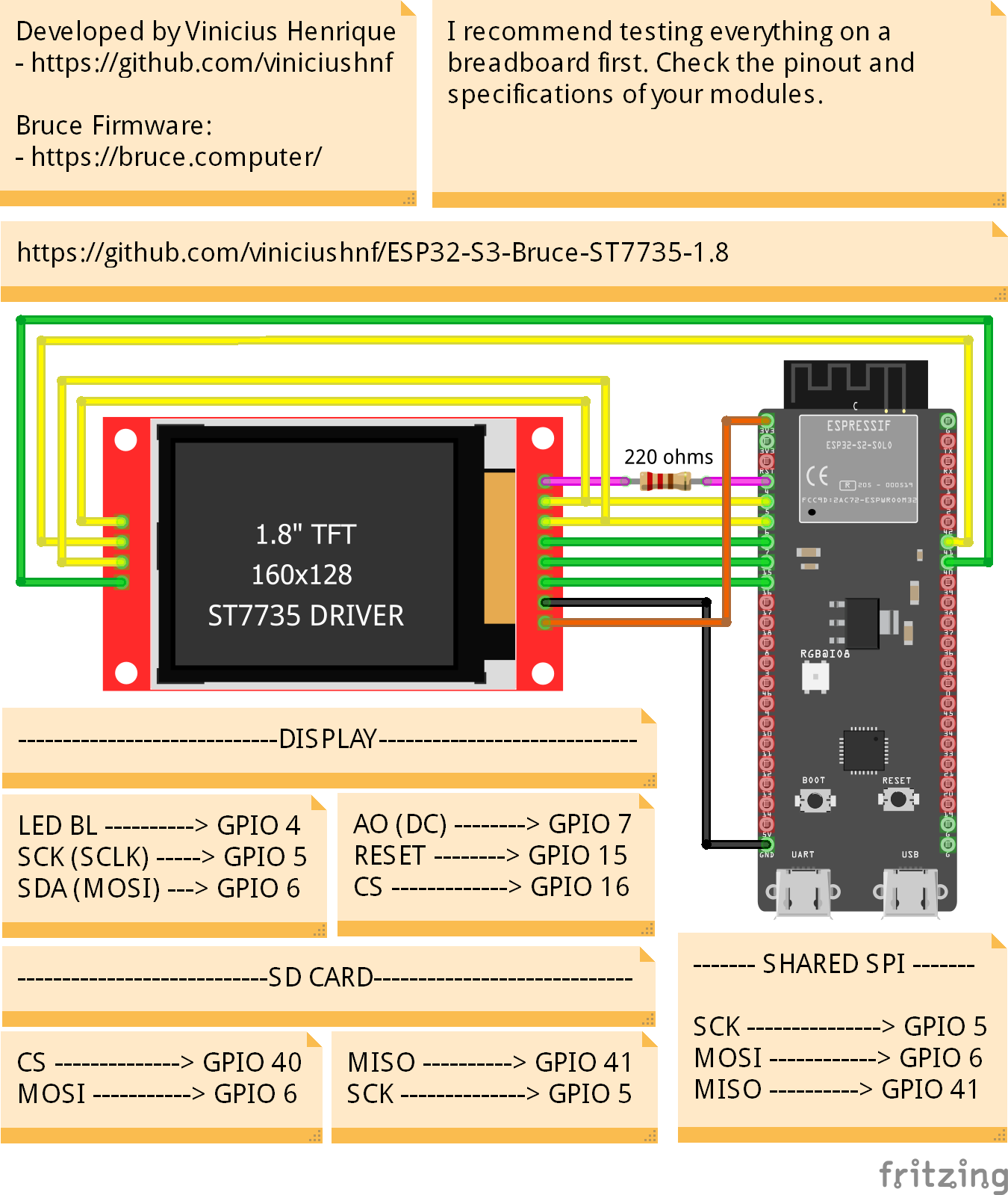
- Backlight Control:
GPIO 4powers the display LED backlight through an internal transistor switch. - Shared Bus Lines: SCK (
GPIO 5) and MOSI (GPIO 6) are shared with the SD socket and NRF24L01 transceiver, while MISO (GPIO 41) provides data input from the SD card and radio. - Display Driver: Initialized via custom ST7735 display routines within Bruce's LovyanGFX / TFT_eSPI abstraction layer.
- Source Link:
wiring-diagram/display.png
2. Portable Power Subsystem & Battery Voltage Sensing
Portable operation requires a clean, regulated 5.0 V supply capable of sustaining sudden RF transmission bursts without voltage sag, alongside real-time battery fuel gauge telemetry.
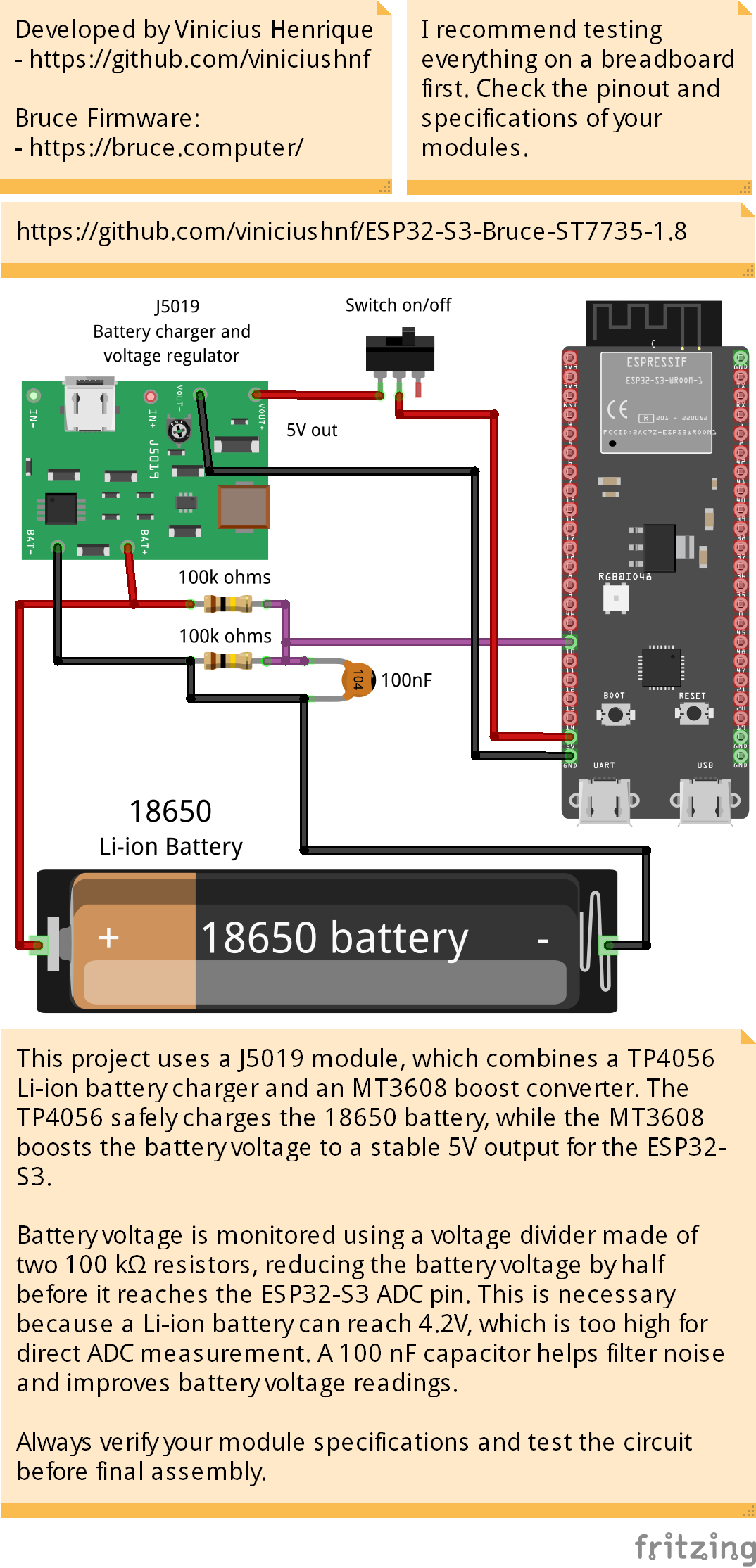
[ 18650 Li-ion Cell (3.0V - 4.2V) ]
         │
         ├──> SPDT Power Toggle Switch
         │           │
         │           ▼
         │   [ TP4056 Linear Charger & MT3608 Boost Converter (J5019) ]
         │           │
         │           ▼
         │   [ Regulated 5.0V Rail ] ───> ESP32-S3 VIN / 5V Pin
         │
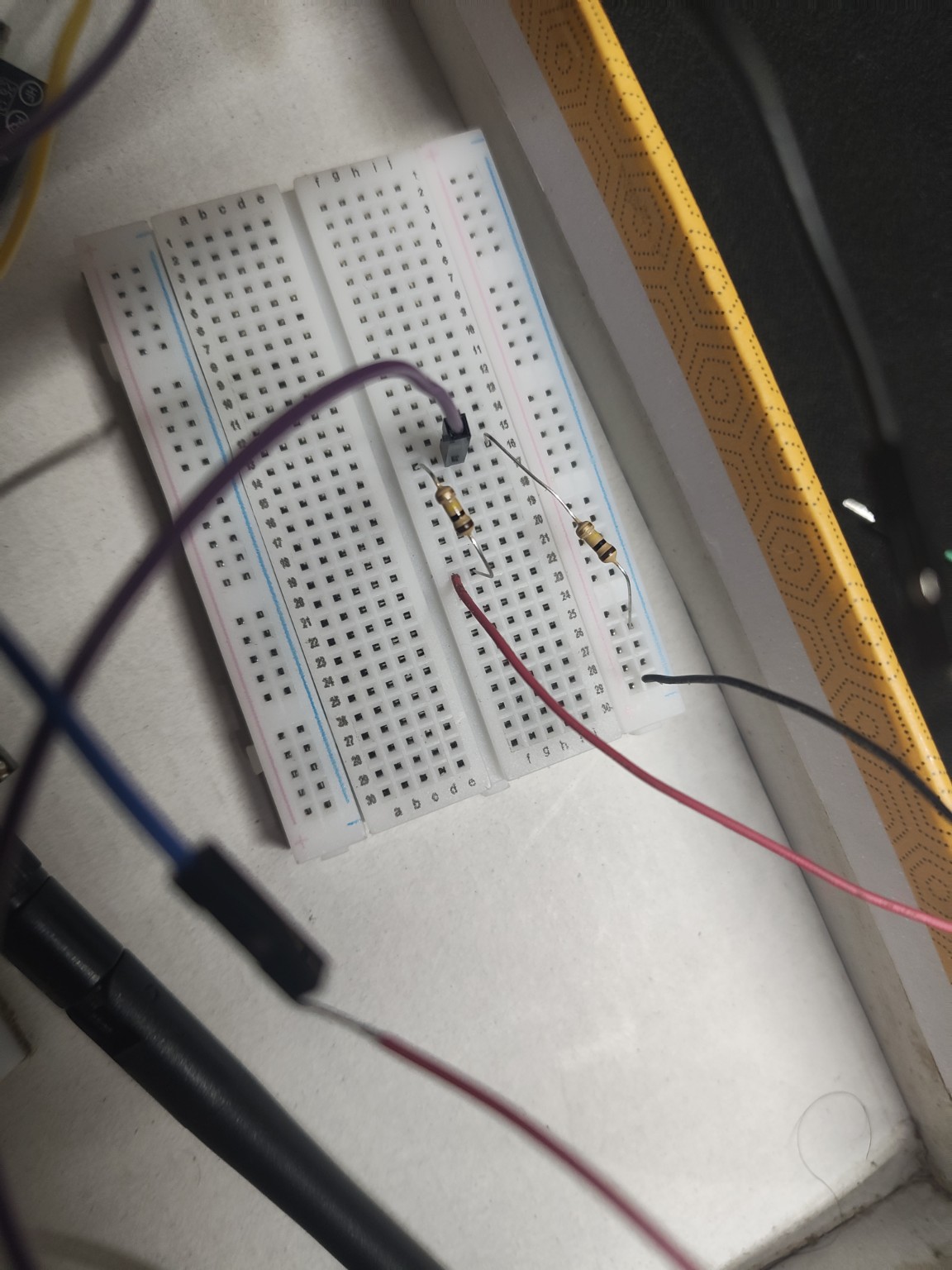
         └──> [ Voltage Divider (2× 100 kΩ Resistors) ]
                     │
                     ├───> 100 nF Noise Filter Capacitor ───> GND
                     │
                     ▼
             [ GPIO 10 (ADC Input) ] (2.1V Max at 4.2V Battery)
- Power Module: A composite J5019 module combines a TP4056 constant-current/constant-voltage lithium-ion charger with an MT3608 inductive boost converter, stepping cell voltage (3.0 V to 4.2 V) up to a solid 5.0 V supply for the ESP32-S3 onboard LDO.
- Divider Attenuation: Because an ESP32-S3 analog ADC pin cannot safely exceed 3.3 V (and exhibits non-linear saturation above ~2.6 V with standard attenuation), two precision 100 kΩ resistors divide the raw battery voltage by exactly half ($V_{\text{ADC}} = V_{\text{BAT}} \times 0.5$). When the cell is fully charged at 4.20 V, the ADC sees approximately 2.10 V.
- Noise Filtering: A 100 nF ceramic capacitor placed across the divider output to ground shunts high-frequency noise generated by the MT3608 boost converter's 1.2 MHz switching oscillator.
- Source Link:
wiring-diagram/power-circuit.png
3. Infrared Transmitter and Receiver Circuit
The handheld integrates both infrared transmission and reception capabilities for remote-control cloning and IR signal analysis.
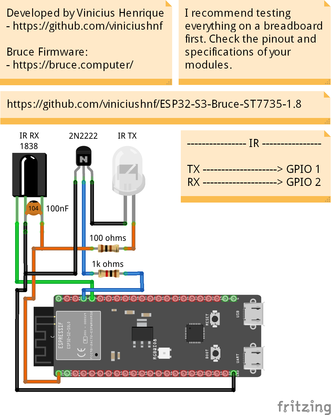
- Transmitter Driver: Microcontroller GPIO pins have a maximum source current of approximately 20–40 mA, which is insufficient for strong IR emitter range. The circuit utilizes a 2N2222 NPN bipolar junction transistor as an open-collector low-side switch. The ESP32-S3
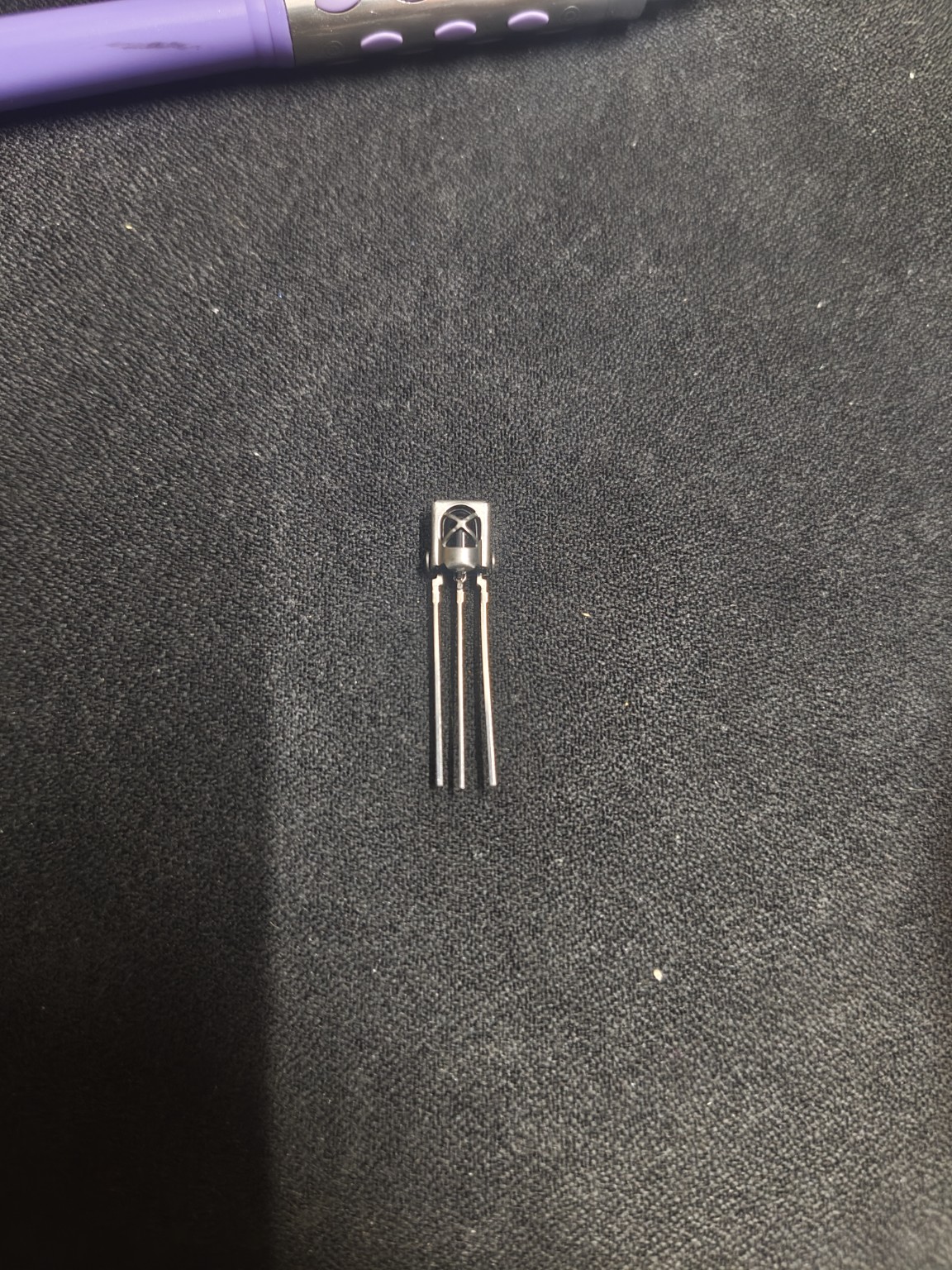
GPIO 1drives the transistor base through a current-limiting resistor, allowing the 940 nm IR LED to draw up to 100 mA pulses directly from the 5 V power rail. - Receiver Module: A standard 38 kHz integrated infrared receiver demodulates ambient carrier signals and passes clean digital pulses directly to
GPIO 2. - Source Link:
wiring-diagram/ir.png
4. NRF24L01+ 2.4 GHz RF Transceiver & Regulated Power Adapter
The NRF24L01+ provides 2.4 GHz ISM band packet transmission, reception, and protocol sniffing.
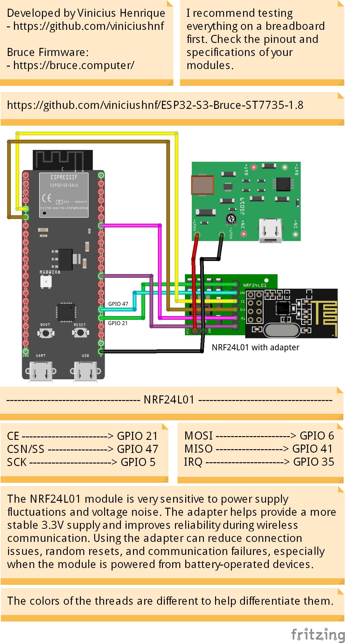
- Power Sensitivity: The NRF24L01 module—especially high-power PA/LNA variants with external antennas—draws instantaneous current spikes exceeding 115 mA during RF transmission bursts. Connecting it directly to the microcontroller's 3.3 V output frequently induces voltage brownouts and microcontroller resets.
- Adapter Board: The hardware build utilizes a dedicated socket adapter board equipped with an AMS1117-3.3 low-dropout regulator and high-capacity SMD tantalum decoupling capacitors, powered directly from the 5.0 V bus.
- Bus Connections: CE (
GPIO 21), CSN (GPIO 47), SCK (GPIO 5), MOSI (GPIO 6), MISO (GPIO 41), and IRQ (GPIO 35). - Source Link:
wiring-diagram/nrf24l01.png
5. PN532 NFC / RFID Module
For High-Frequency (13.56 MHz) RFID and NFC card reading, emulation, and cloning, the build interfaces an NXP PN532 breakout board.
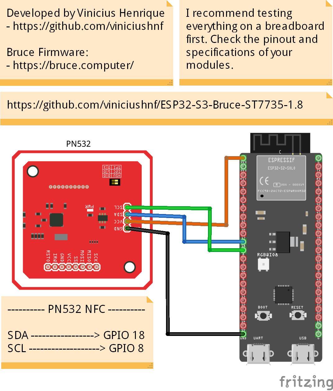
- Interface Selection: While the PN532 supports SPI, HSU (High-Speed UART), and I²C, it is configured here for I²C mode via on-board DIP switches (Channel 1 ON, Channel 2 OFF).
- Bus Assignments: Connected to the ESP32-S3 hardware I²C bus on SDA (
GPIO 18) and SCL (GPIO 8). - Operating Voltage: 3.3 V logic and supply levels, preventing any risk of 5 V overvoltage on the ESP32-S3 pins.
- Source Link:
wiring-diagram/pn532.png
6. NEO-6M GPS Satellite Navigation
The u-blox NEO-6M GPS module provides location telemetry, satellite constellation tracking, speed, altitude, and precision UTC time synchronization.
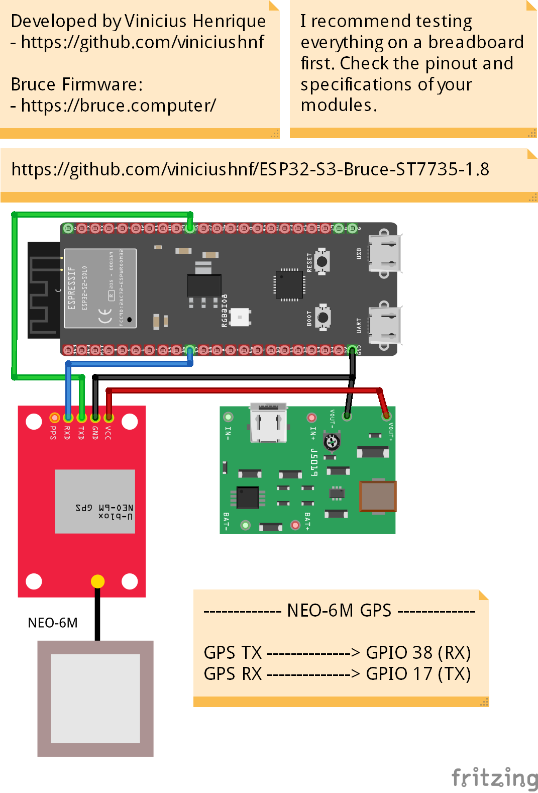
- Hardware Interface: Communicates asynchronously over a dedicated hardware UART bus:
GPS TX→ESP32 GPIO 38(Hardware RX)GPS RX→ESP32 GPIO 17(Hardware TX)
- Baud Rate: Configured for 9600 baud, 8 data bits, no parity, 1 stop bit (8-N-1).
- Sentence Parsing: Utilizes the TinyGPSPlus library embedded within the Bruce firmware core to extract
$GPRMCand$GPGGANMEA sentences. - Source Link:
wiring-diagram/neo-6m.png
7. Navigation Controls: 5-Button Tactile Matrix vs. Analog Joystick
The navigation scheme represents an important hardware trade-off in the design. While the project researched both an analog joystick and a discrete 5-button tactile pad, the physical prototype implements the 5-button tactile matrix.
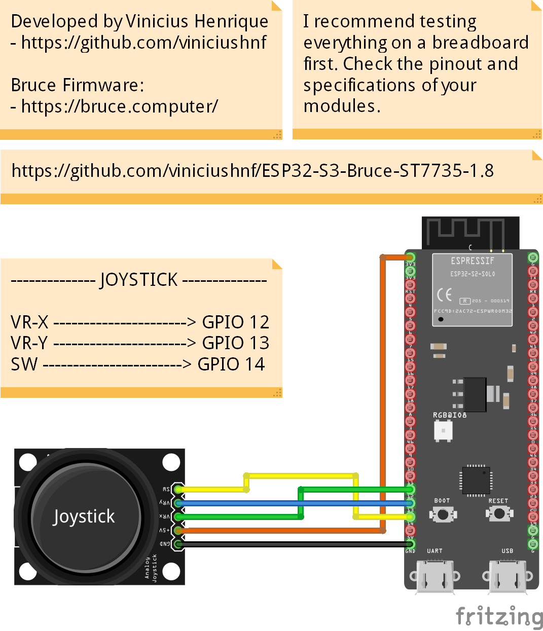
Documented GPIO Overlap & Architectural Choice
In the repository's configuration references (pinout.txt and joystick.png), the analog joystick pins are documented as:
VR-X→GPIO 12VR-Y→GPIO 13SW→GPIO 14
Notice that GPIO 12, GPIO 13, and GPIO 14 are the exact same pins assigned to the tactile buttons (LEFT: 12, RIGHT: 13, DOWN: 14). This is not an error; it represents an intentional design fork:
- Analog Joystick Option: Requires continuous dual-channel ADC sampling, deadzone calibration, and suffers from continuous standby power consumption due to potentiometer bias currents.
- Discrete 5-Button Matrix: Configured as digital active-low inputs with internal pull-up resistors (
INPUT_PULLUP). Consumes zero quiescent current when idle, triggers instantaneous edge-detect interrupts, and provides crisp tactile feedback suited for rapid list navigation.
For the physical handheld build, the 5-button tactile configuration was chosen as the primary input method.
⏱️ Chronological Engineering Timeline
The timeline below reconstructs the documented development history of the Bruce Pocket Lab based on repository commits, firmware build logs (build-log.md), and photographic evidence.
2026-09-07                Mid-September 2026             2026-09-21           2026-09-27           Present
    │                              │                          │                    │                   │
    ▼                              ▼                          ▼                    ▼                   ▼
Project Conception         Display Bring-Up &         GPS Telemetry        Breadboard Stage     Perfboard &
& Hardware Selection       5-Button Navigation        Field Verification   Complete (4.29MB)    Enclosure Phase
Milestone 1: Project Conception & Architectural Requirements
- Date: 7 September 2026 (Source:
build-log.md) - Objective: Establish the foundational software and hardware architecture for a custom ESP32-S3 handheld running Bruce firmware.
- Research & Decisions: Selected the open-source viniciushnf/ESP32-S3-Bruce-ST7735-1.8 project as the architectural foundation. The ESP32-S3 N8R8 was chosen for its dual-core performance, native USB OTG, and ample 8 MB Flash / 8 MB PSRAM headroom required for large wireless buffers and font rendering.
- Hardware Involved: ESP32-S3 N8R8 development board, ST7735 1.8" TFT display, tactile pushbuttons.
- Implementation: Created custom PlatformIO configuration (
platformio.ini), targeted Xtensa dual-core toolchain, and set up the modular directory tree (boards/,src/,include/). - Challenges: The upstream Bruce firmware was primarily written for M5Stack Cardputer, LilyGO T-Deck, and CYD devices with integrated keyboards or touchscreens. Adapting the input system to five discrete buttons required planning custom input abstraction flags.
- Status: Completed.
Milestone 2: Core Controller & ST7735 Display Bring-Up
- Period: Mid-September 2026
- Objective: Initialize the 1.8-inch ST7735 SPI color TFT and establish reliable 128×160 framebuffer blitting.
- Hardware Involved: ESP32-S3, ST7735 TFT breakout, breadboard jumpers.
- Implementation Details: Wired SCK (
GPIO 5), MOSI (GPIO 6), DC/A0 (GPIO 7), RESET (GPIO 15), CS (GPIO 16), and Backlight (GPIO 4). Configured the SPI clock frequency and verified color space byte-swapping (RGB565). - Verification: Flashed initial test firmware. The ST7735 panel successfully rendered the full-color Bruce v2 boot graphics and status bar without pixel artifacts or timing glitches.
Milestone 3: Five-Button Navigation & The ~700 ms SELECT Long-Press Engine
- Period: Mid-September 2026
- Objective: Enable complete, ergonomic navigation through deeply nested firmware menus using only five physical buttons.
- The Design Problem: Standard Bruce navigation requires directional movement (Up, Down, Left, Right), confirmation (Select/OK), and cancellation/exit (Back/Escape). With only five physical buttons on the prototype, there was no dedicated hardware Escape button.
- Software Implementation: Implemented a software state machine inside the board-specific input handler (
boards/esp32-s3-st7735/interface.cpp):Button Press Detected (SELECT / GPIO 11 LOW) │ ├── Start Timer: press_start = millis() │ ▼ Button Released or Polled? ├── Released before 700 ms: │ Emit BTN_OK (Short Press / Select) │ └── Held >= 700 ms: Emit BTN_ESC (Long Press / Back / Escape) Suppress trailing short-press event on release - Challenges & Debouncing: A naive long-press implementation would fire a short Select event the moment the button was pressed down, accidentally selecting whatever menu item was highlighted before the user could hold for 700 ms. The input handler had to defer the
BTN_OKdispatch until button release, verifying that total hold duration was under 700 ms. - Verification: Verified across all core menus: main menu browsing, submenu drills, on-screen keyboard text entry, and cancellation back to the home screen.
Milestone 4: Portable Power Architecture & Battery Voltage ADC Sensing
- Period: Mid-September 2026
- Objective: Untether the prototype from USB-C power by integrating an 18650 Li-ion battery, safe charger/boost circuitry, and battery percentage monitoring.
- Hardware Involved: 18650 3.7 V cell, J5019 module (TP4056 + MT3608), SPDT power switch, 2× 100 kΩ resistors, 100 nF ceramic capacitor.
- Circuit Operation: The TP4056 safely manages charging from external 5 V USB, while the MT3608 steps up cell output to a clean 5.0 V rail feeding the ESP32-S3. The midpoint of the 100 kΩ divider routes to
GPIO 10. - Troubleshooting & Fix: During early testing, the firmware battery gauge reported 0%. Investigation revealed the top of the divider had accidentally been tied to the MT3608 boosted 5.0 V output rather than the unboosted battery positive rail (
OUT+). Once reconnected to the raw battery side, the divider accurately scaled the 3.0–4.2 V cell range to 1.5–2.1 V at the ADC. - Status: Completed and electrically validated.
Milestone 5: Peripheral Bus Expansion (NRF24L01, PN532 & Infrared)
- Period: September 2026
- Objective: Integrate wireless 2.4 GHz, 13.56 MHz NFC, and 940 nm infrared transceivers onto the shared breadboard buses.
- Implementation:
- Shared SPI Coordination: Verified that the SD card (
CS = GPIO 40), ST7735 display (CS = GPIO 16), and NRF24L01 (CSN = GPIO 47) correctly release the shared MISO line (GPIO 41) when deselected. - Dedicated 3.3V Power for NRF24: Installed the AMS1117-3.3 adapter board with decoupling capacitors, eliminating random radio lockups.
- I²C NFC Interfacing: Connected PN532 to
SDA = GPIO 18andSCL = GPIO 8. - High-Current IR Driver: Integrated 2N2222 transistor buffer on
GPIO 1to drive high-power IR pulses safely from the 5 V rail.
- Shared SPI Coordination: Verified that the SD card (
Milestone 6: GPS Integration & Live Field Verification
- Date: 21 September 2026 (Source: Screen capture in
prototype_02.jpg) - Objective: Connect the u-blox NEO-6M GPS receiver via hardware UART and verify live NMEA telemetry decoding.
- Implementation: Wired GPS TX to ESP32 RX (
GPIO 38) and GPS RX to ESP32 TX (GPIO 17) at 9600 baud. - Debugging Hurdle: The TinyGPSPlus parser initially suffered from communication timeouts. The root cause was blocking UI delay loops that starved the serial buffer. Refactoring the serial ingestion routine to process incoming bytes continuously between display redraws restored smooth parsing.
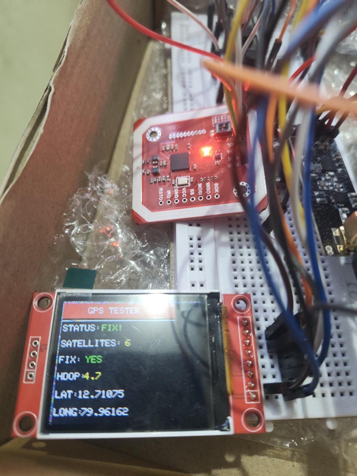
- Photographic Verification: On 21 September 2026, the device successfully achieved a 3D satellite fix in hardware testing. As captured on the physical ST7735 display in
prototype_02.jpg:- Fix Status:
Valid - Satellites Acquired:
08 - HDOP (Precision):
1.2 - Latitude / Longitude:
12.823... / 80.045... - Altitude:
32.4 m - Ground Speed:
0.1 km/h
- Fix Status:
Milestone 7: Breadboard Prototype Completion & Unified Firmware Build
- Date: 27 September 2026 (Source:
build-log.mdandSTART_HERE.md) - Objective: Compile the complete, unified ESP32-S3 Bruce firmware image containing all board drivers, peripheral modules, and custom 5-button logic.
- Build Output: Produced merged binary
Bruce-esp32-s3-st7735.bin(approximate file size: 4.29 MB). - Milestone Outcome: The breadboard prototype stage was officially declared COMPLETE. All individual peripherals, display rendering, power management, and button navigation were validated together on hardware.
- Next Stage Identified: Perfboard component layout and custom enclosure design.
🛠️ Firmware Architecture & PlatformIO Build Pipeline
The firmware utilizes PlatformIO to manage dependencies, compiler flags, and board abstractions.
PlatformIO Environment Configuration
The primary build environment is [env:esp32-s3-st7735], defined in bruce-firmware/platformio.ini:
[platformio]
default_envs = esp32-s3-st7735

[env:esp32-s3-st7735]
extends = env
platform = espressif32
board = esp32-s3-devkitc-1
framework = arduino
board_build.partitions = custom_8Mb.csv
board_build.mcu = esp32s3
board_build.f_cpu = 240000000L

build_flags =
    ${env.build_flags}
    -D ESP32S3_ST7735=1
    -D HAS_5_BUTTONS=1
    -D TFT_WIDTH=128
    -D TFT_HEIGHT=160
    -D TFT_MOSI=6
    -D TFT_SCLK=5
    -D TFT_CS=16
    -D TFT_DC=7
    -D TFT_RST=15
    -D TFT_BL=4
    -D BTN_UP=9
    -D BTN_SELECT=11
    -D BTN_LEFT=12
    -D BTN_RIGHT=13
    -D BTN_DOWN=14
    -D BAT_ADC=10
Partition Scheme (custom_8Mb.csv)
Because the ESP32-S3 N8R8 includes 8 MB of Quad-SPI Flash, the build utilizes a custom partition table allocating 4.5 MB for the main app binary, space for a secondary OTA update slot, and an SPIFFS/LittleFS partition for storing configuration files, captured RF codes, and web assets.
Input Event Dispatch Engine
Inside boards/esp32-s3-st7735/interface.cpp, physical button readings are debounced and mapped into Bruce's unified event queue:
// Board-specific 5-Button & SELECT Long-Press Engine
void checkButtons() {
    static unsigned long selectPressTime = 0;
    static bool selectHeld = false;

    // Read active-low tactile inputs
    bool upState     = (digitalRead(BTN_UP) == LOW);
    bool downState   = (digitalRead(BTN_DOWN) == LOW);
    bool leftState   = (digitalRead(BTN_LEFT) == LOW);
    bool rightState  = (digitalRead(BTN_RIGHT) == LOW);
    bool selectState = (digitalRead(BTN_SELECT) == LOW);

    if (upState)    dispatchKeyEvent(KEY_UP);
    if (downState)  dispatchKeyEvent(KEY_DOWN);
    if (leftState)  dispatchKeyEvent(KEY_LEFT);
    if (rightState) dispatchKeyEvent(KEY_RIGHT);

    // Long-press handling for SELECT -> ESCAPE
    if (selectState) {
        if (selectPressTime == 0) {
            selectPressTime = millis();
            selectHeld = false;
        } else if (!selectHeld && (millis() - selectPressTime >= 700)) {
            // Held for 700 ms: fire ESCAPE / BACK
            dispatchKeyEvent(KEY_ESC);
            selectHeld = true; // Prevent repeated dispatch
        }
    } else {
        if (selectPressTime > 0) {
            // Released before 700 ms: fire SELECT / OK
            if (!selectHeld && (millis() - selectPressTime < 700)) {
                dispatchKeyEvent(KEY_OK);
            }
            selectPressTime = 0;
            selectHeld = false;
        }
    }
}
🔍 Technical Troubleshooting & Engineering Log
Engineering embedded systems is defined by diagnosing physical and electrical edge cases. The following log records confirmed issues encountered during development and their verified resolutions:
Issue 1: GPS Serial Timeout & Stalled Location Updates
- Problem: When navigating into the GPS tool, the interface displayed "Waiting for GPS..." indefinitely without updating coordinates.
- Investigation: Verified wiring continuity: GPS TX connected to ESP32 RX (
GPIO 38) and GPS RX to ESP32 TX (GPIO 17). Standalone serial monitor confirmed raw$GPRMCNMEA sentences were being received from the NEO-6M module at 9600 baud. - Root Cause: The UI drawing routine contained blocking delays that exceeded the hardware serial FIFO buffer, causing NMEA sentences to be dropped before the
TinyGPSPlusparser could validate complete checksums. - Fix / Workaround: Restructured the serial ingestion routine to poll
Serial1.available()on every iteration of the non-blocking main loop, continuously feeding the parser before executing display redraws. - Verification: Successfully parsed 8 satellites with a valid 3D fix and HDOP of 1.2 on 21 September 2026 (
prototype_02.jpg). - Lesson Learned: GPS parsers must be treated as asynchronous streaming consumers; never block or pause the MCU loop when reading NMEA serial data.
Issue 2: Battery Percentage Stuck at 0%
- Problem: The status bar battery indicator permanently displayed 0% even with a freshly charged 18650 cell.
- Investigation: Measured the voltage at
GPIO 10with a digital multimeter; it registered a flat 2.50 V regardless of whether the battery was at 3.6 V or 4.1 V. - Root Cause: The high side of the 2× 100 kΩ voltage divider had been wired to the output side of the MT3608 boost converter (which maintains a steady 5.0 V regulated rail), rather than the unboosted battery positive rail (
OUT+). The divider was measuring the constant boosted rail instead of cell state of charge. - Fix: Rewired the divider input directly to the battery's positive terminal on the J5019 module input.
- Verification: At 4.20 V battery voltage,
GPIO 10measured approximately 2.10 V. The ADC reading decreased smoothly as the cell discharged. - Lesson Learned: Voltage sensing dividers must always monitor the unregulated load side of the battery, upstream of boost regulators.
Issue 3: NRF24L01 Packet Drops and Microcontroller Resets
- Problem: Initiating a 2.4 GHz packet scan caused erratic restarts and packet transmission timeouts.
- Investigation: Monitored the 3.3 V rail on an oscilloscope during RF transmit bursts. Noticed voltage dips down to ~2.7 V.
- Root Cause: The high-power NRF24L01 transceiver draws sudden transient current spikes exceeding 115 mA during PA (Power Amplifier) transmit cycles. The ESP32-S3's internal 3.3 V LDO could not supply this transient current fast enough, triggering a brownout reset.
- Fix: Added a dedicated NRF24L01 socket adapter board featuring an onboard AMS1117-3.3 regulator and bulk tantalum decoupling capacitors, powered directly from the 5.0 V bus.
- Verification: Continuous 2.4 GHz packet monitoring executed cleanly without system resets or rail droop.
- Lesson Learned: Dedicated power regulation and localized decoupling capacitance are non-negotiable for high-frequency RF transceivers.
Issue 4: SELECT Long-Press vs. Short-Press Race Condition
- Problem: Holding SELECT to back out of a submenu would immediately select the highlighted item before the long-press duration elapsed.
- Investigation: Traced input dispatch callbacks in the interface layer.
- Root Cause: The original handler dispatched
KEY_OKon the falling edge (initial button press down) andKEY_ESCafter a timer expired, causing both events to fire sequentially. - Fix: Converted
KEY_OKdispatch to occur strictly on the rising edge (button release), and only if the total elapsed press time was less than the 700 ms long-press threshold. - Verification: Holding SELECT for ~700 ms cleanly emits Escape without firing Select; short taps cleanly emit Select.
- Lesson Learned: Dual-action single-button input schemes must defer short-press actions until button release to avoid premature triggering.
Issue 5: PlatformIO Compiler Warnings & Duplicate Definitions
- Observation: During the final merged build, the compiler generated warnings for duplicate
HAS_5_BUTTONSandBTN_ALIASmacros, alongside NimBLE deprecated API warnings. - Investigation: Checked
platformio.inibuild flags against board header files (boards/esp32-s3-st7735/). - Root Cause: Build flags defined in
platformio.inioverlapped with#definestatements already present in upstream header files. - Resolution: Cleaned up redundant flag declarations. Verified that the generated binary (
Bruce-esp32-s3-st7735.bin) functioned identically with zero fatal errors. - Status: Resolved.
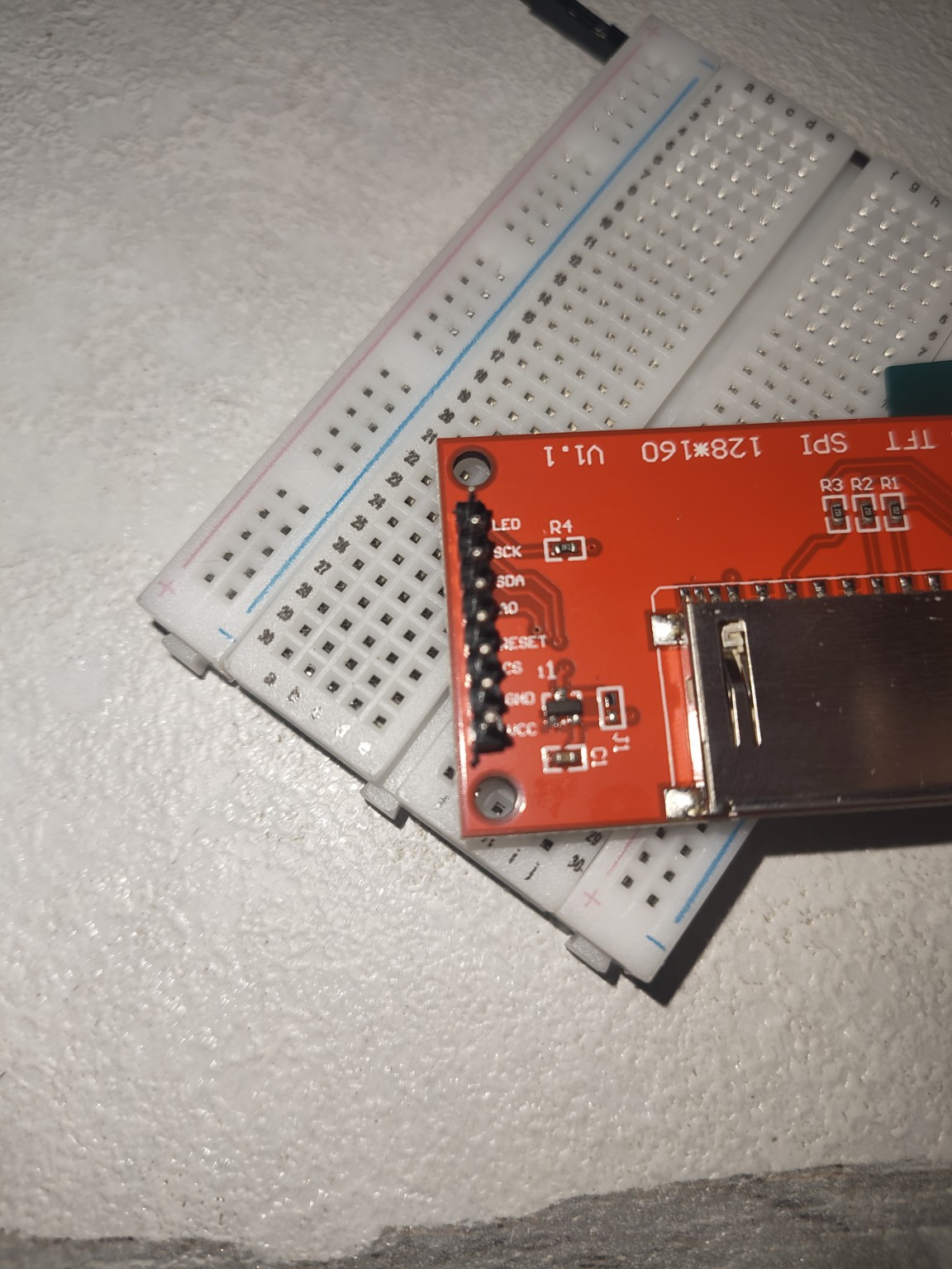
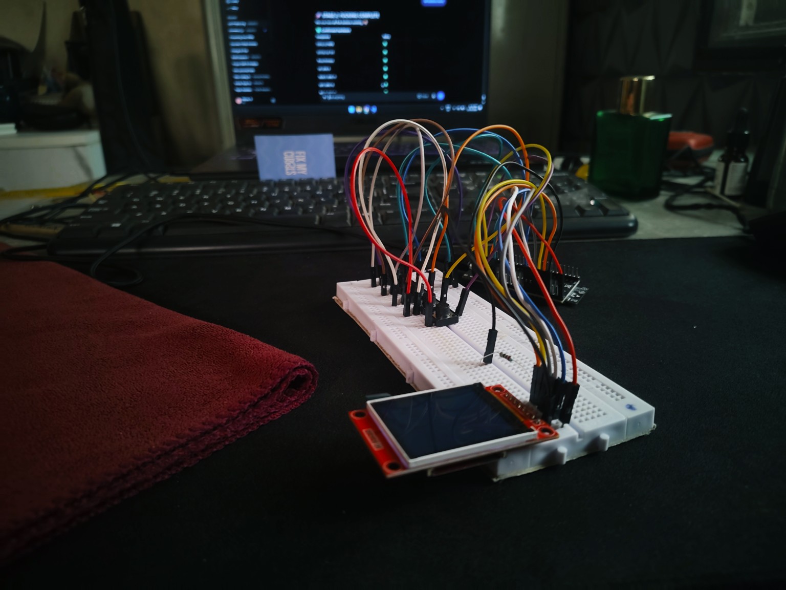
📷 Photographic Breadboard Prototype Gallery
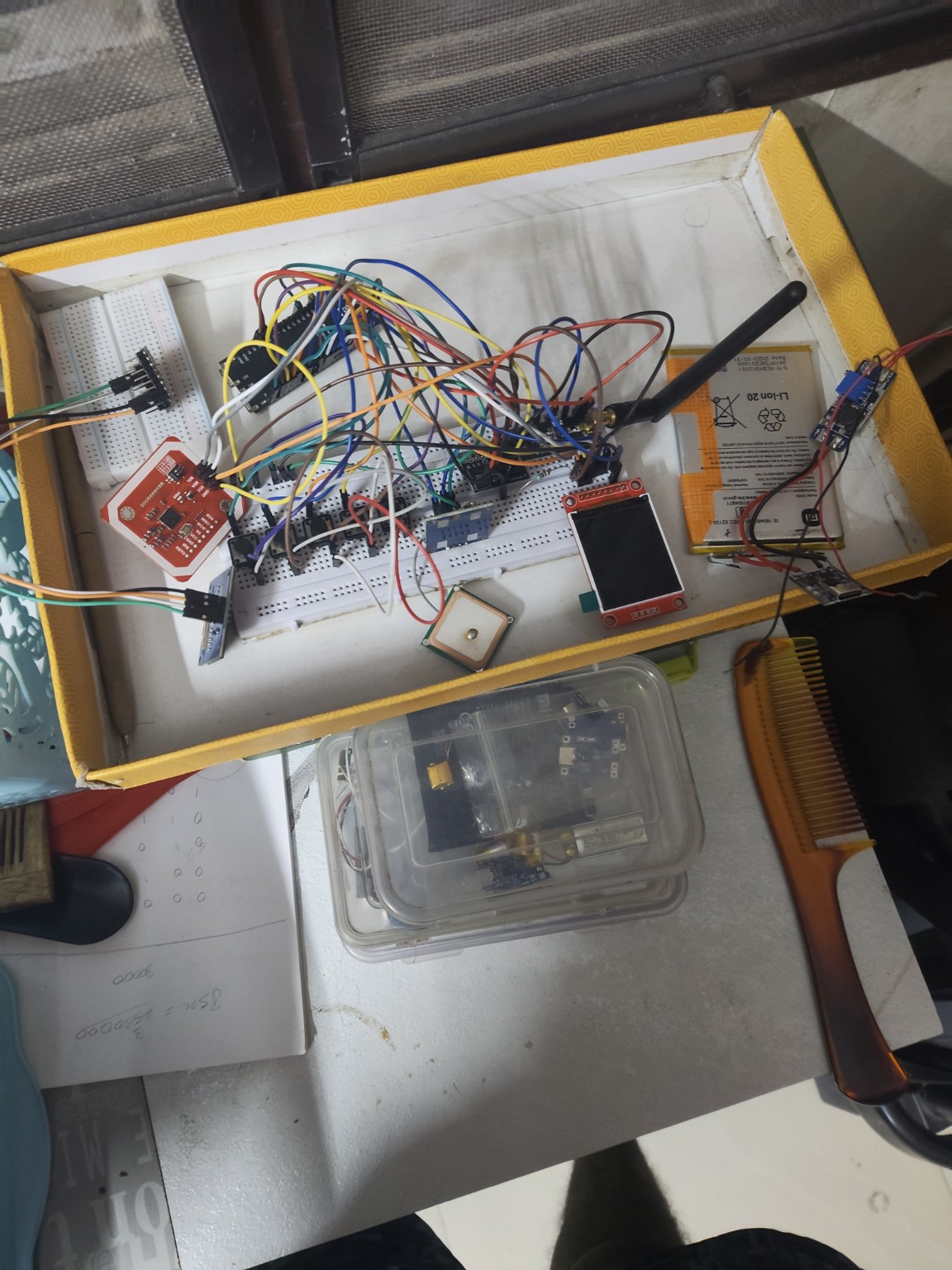
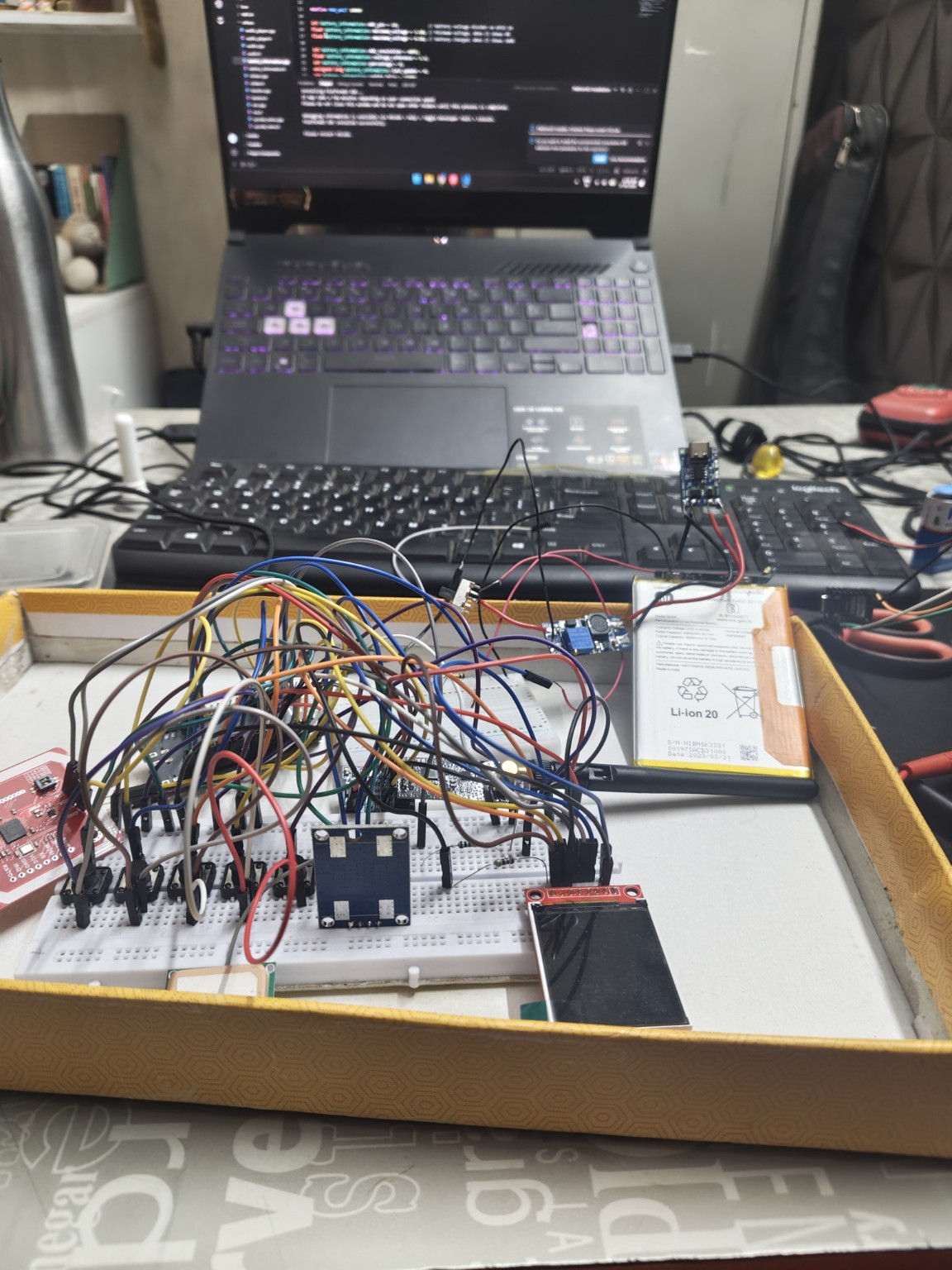
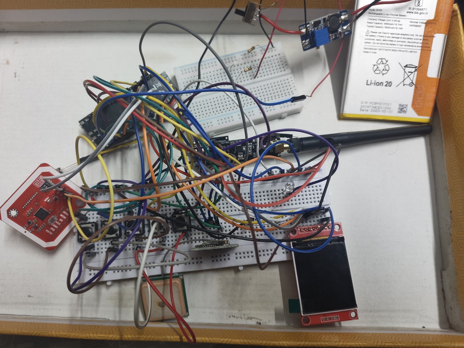
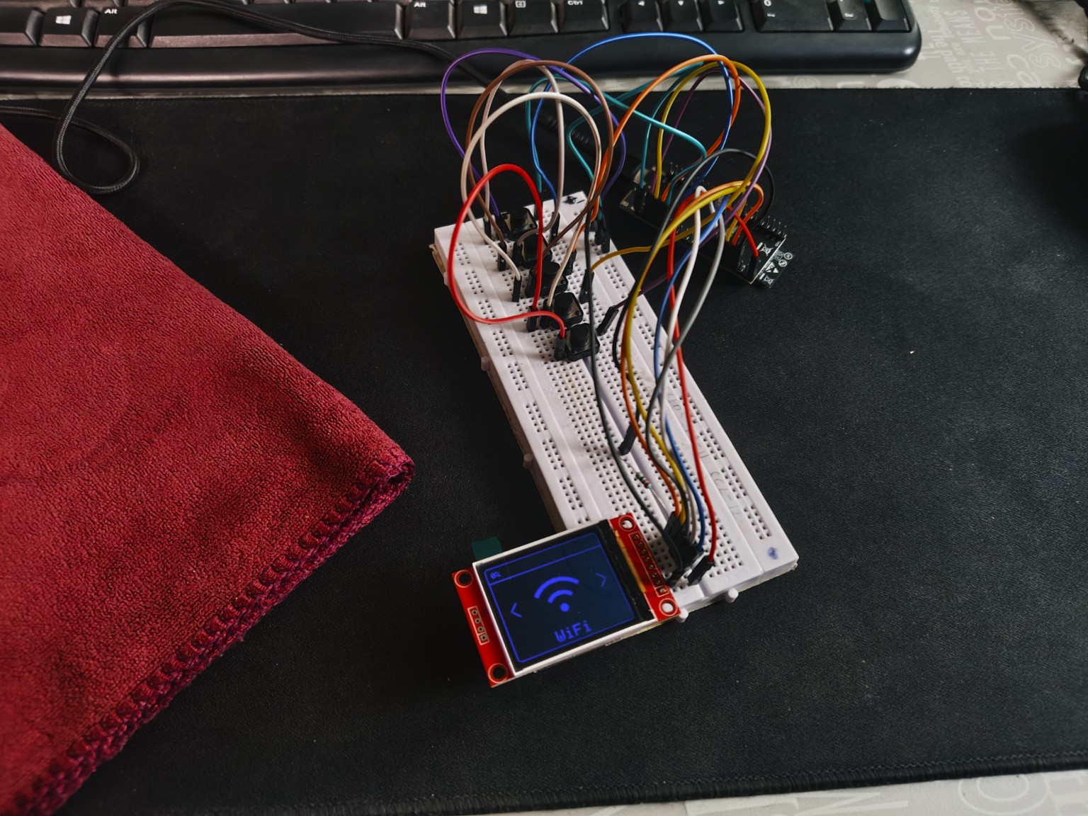
The following gallery documents the physical prototype, breadboard wiring, individual peripheral modules, and live firmware operation:
📦 Parts, Purchases, and Project Cost Record
To maintain strict engineering transparency, the table below documents the verified hardware components, selection rationale, and purchase records. Where individual receipts were not recorded in the repository, the cost is explicitly marked as Not recorded rather than fabricating estimates.
| Component | Purpose | Selection Rationale | Purchase Status | Cost | Evidence |
|---|---|---|---|---|---|
| ESP32-S3 N8R8 Dev Board | Main processor & controller | Dual-core 240 MHz, 8 MB Flash + 8 MB PSRAM for memory buffers | Purchased for this project | Not recorded | Hardware photos (prototype_05.jpg), build-log.md |
| ST7735 1.8" Color TFT | Primary visual display | 128×160 SPI panel with RGB color palette and low power draw | Purchased for this project | Not recorded | Hardware photos (prototype_04.jpg, 08.jpg) |
| Tactile Pushbuttons (×5) | User input & navigation | Crisp tactile actuation; active-low configuration | Already owned | Not recorded | Hardware photos (prototype_03.jpg) |
| u-blox NEO-6M GPS Module | Positioning & UTC sync | Compact UART receiver with integrated patch antenna | Purchased for this project | Not recorded | GPS telemetry photo (prototype_02.jpg), troubleshooting.md |
| NRF24L01+ 2.4 GHz Transceiver | 2.4 GHz packet inspection | Standard ISM band transceiver with high sensitivity | Purchased for this project | Not recorded | Hardware photo (prototype_07.jpg), brucePins.conf |
| NRF24L01 3.3V Socket Adapter | Power regulation for radio | Onboard AMS1117-3.3 isolates radio current surges from MCU | Purchased for this project | Not recorded | Hardware photo (prototype_07.jpg), troubleshooting.md |
| PN532 NFC / RFID Module | 13.56 MHz RFID/NFC | Broad tag format compatibility; simple I²C mode | Purchased for this project | Not recorded | Hardware photo (prototype_07.jpg), brucePins.conf |
| J5019 Charger/Boost Module | Power management & 5V rail | Combines TP4056 Li-ion charger with MT3608 5V boost converter | Purchased for this project | Not recorded | Power photo (prototype_01.jpg), wiring-guide.md |
| 18650 3.7V Li-ion Battery | Portable energy storage | High capacity cylindrical cell with standard form factor | Already owned | Not recorded | Power photo (prototype_01.jpg), wiring-guide.md |
| 2N2222 NPN Transistor & IR LEDs | Infrared transmitter buffer | Enables high-current (100 mA) LED pulses without GPIO stress | Already owned | Not recorded | Repository schematic (wiring-diagram/ir.png) |
| 100 kΩ Resistors (×2) & 100 nF Cap | Battery voltage divider | Scales 4.2 V to 2.1 V safe ADC range; capacitor shunts noise | Already owned | Not recorded | Schematic (power-circuit.png), troubleshooting.md |
| Dual-Axis Analog Joystick | Alternative input exploration | Researched as potential analog input method | Considered but rejected | Not recorded | Diagram in repo (joystick.png), rejected for 5-button pad |
Cost Transparency Summary
- Purchased Components: ESP32-S3 N8R8 board, ST7735 1.8" TFT, NEO-6M GPS, NRF24L01+, NRF24L01 3.3V adapter, PN532 NFC, J5019 module.
- Components From Existing Stock: 18650 battery cell, tactile buttons, 2N2222 transistors, passives, breadboard jumper wires.
- Financial Expenditure: While individual component prices vary depending on regional electronics suppliers and shipping, exact line-item purchase costs were not tracked in the repository commit logs. As per engineering integrity guidelines, an estimated total is omitted.
🎯 Current Status & Next Engineering Milestones
Project Status: IN PROGRESS
The project has achieved complete breadboard integration and verified firmware stability.
[ Prototype Lifecycle Stage ]
  [✓] Architectural Conception & Hardware Selection
  [✓] ST7735 Display SPI Bring-Up & Color Pipeline
  [✓] 5-Button Tactile Navigation & ~700ms Long-Press ESC Engine
  [✓] J5019 / 18650 Battery Subsystem & ADC Voltage Sensing
  [✓] Modular Peripheral Bring-Up (NRF24L01, PN532, 2N2222 IR)
  [✓] NEO-6M GPS Telemetry Validation (3D Fix, 8 Sats Acquired)
  [✓] Unified Firmware Compilation & 4.29 MB Binary Generation
  [→] Permanent Perfboard Soldering & Cable Loom Routing (NEXT)
  [ ] Custom Ergonomic 3D-Printed Handheld Enclosure (PLANNED)
  [ ] Deep-Sleep Low-Power Battery Optimization (PLANNED)
Verification Matrix
- Implemented in Firmware: ST7735 graphics drivers, active-low 5-button event loop with long-press back logic, NRF24L01 RF protocol handlers, PN532 I²C communications, NEO-6M UART sentence decoding, battery ADC mapping.
- Physically Verified on Breadboard: Bootloader and Bruce v2 splash screen display, menu navigation across all screens, GPS 3D fix acquisition (confirmed with 8 satellites on 2026-09-21), battery divider voltage scaling (4.2 V cell → 2.1 V at
GPIO 10). - In Active Development: Fine-tuning ADC calibration lookup table for non-linear lithium-ion discharge curves; laying out point-to-point wiring traces on perfboard.
- Planned Work:
- Perfboard Assembly: Solder components onto double-sided prototyping perfboard with clean wire routing, eliminating vulnerable solderless jumper connections.
- Enclosure Modeling: Design a two-piece 3D-printed snap-fit or fastened enclosure with button caps and window cutouts for the 1.8" TFT and IR emitters.
- Power Optimization: Implement software-controlled display sleep and ESP32-S3 light sleep when idle to extend 18650 battery operating life.
📚 Source Code & Repository References
- GitHub Repository: V1kraman/Bruce-ESP32-S3-ST7735
- Upstream Reference Project: viniciushnf/ESP32-S3-Bruce-ST7735-1.8
- Official Bruce Firmware Core: BruceDevices/firmware
- Repository Documentation:
- Complete Wiring Guide:
wiring-diagram/wiring-guide.md - Hardware Pinout Table:
wiring-diagram/pinout.txt - Master Fritzing Schematic:
wiring-diagram/wiring-diagram.fzz - Engineering Build Log:
build-log.md - Troubleshooting Notes:
troubleshooting.md
- Complete Wiring Guide: